Характеристики
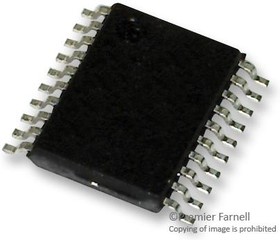
SN74LVC541APW, Буфер / драйвер линии, неинвертирующий …The SN74LVC541APWR is an octal Buffer/Driver with 3-state outputs and designed for 1.65 to 3.6V VCC operation. The device features inputs and outputs facilitate printed circuit board layout. The 3-state control gate is a 2-input AND gate with active-low inputs so that, if either output enable (OE1 or OE2) input is high, all eight outputs are in the high-impedance state. Inputs can be driven from either 3.3/5V devices. This feature allows the use of these devices as translators in a mixed 3.3/5V system environment. This device is fully specified for partial-power-down applications using IOFF. The IOFF circuitry disables the outputs, preventing damaging current backflow through the device when it is powered down. To ensure the high-impedance state during power up or power down, OE should be tied to VCC through a pull-up resistor and the minimum value of the resistor is determined by the current-sinking capability of the driver.
• Support mixed-mode signal operation on all ports
• IOFF Supports partial-power-down mode operation
• Latch-up performance exceeds 250mA per JESD 17
• Inputs accept voltages to 5.5V
• 5.1ns at 3.3V Propagation delay (tpd)
• 2V at VCC = 3.3V, TA = 25°C VOHV (output VOH undershoot)
• Green product and no Sb/Br
 Личный кабинет


 Загрузка